
NVIDIA’s Blackwell architecture is not just an incremental update; it’s a fundamental redesign aimed at solving the biggest bottlenecks in modern AI computing. The sheer size and complexity of today’s largest language models (LLMs) and generative AI applications require a new approach to hardware, and Blackwell delivers this through several key innovations.
Here’s how NVIDIA’s Blackwell architecture enhances AI computing:
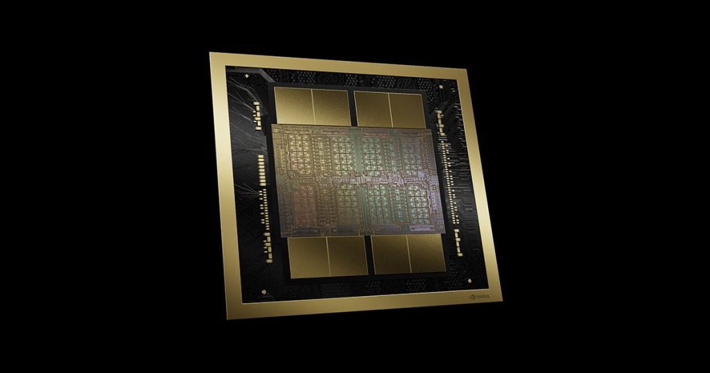
1. A New Paradigm in Chip Design: The Multi-Chip Module (MCM)
Breaking the Monolithic Barrier: Previous high-end GPUs like the Hopper H100 were monolithic, meaning all the cores and components were on a single, massive die. This approach is reaching its physical limits due to the high cost and low yield of manufacturing extremely large chips.
Unified Dual-Die Design: Blackwell, in a revolutionary move for a consumer-grade GPU, combines two separate GPU dies into a single package. These two dies are connected by a high-speed, 10 TB/s NV-High Bandwidth Interface (NV-HBI). This allows the two chips to act as a single, cohesive GPU with a unified memory space and cache, effectively doubling the compute resources while avoiding the manufacturing limitations of a single, giant chip.
2. Unprecedented Performance and Efficiency
FP4 Precision for Inference: Blackwell introduces native hardware support for a new 4-bit floating-point (FP4) format. This is a game-changer for AI inference, as it significantly reduces the memory footprint of a model and doubles the throughput compared to the 8-bit precision (FP8) used in Hopper. This means you can run larger, more complex models with less memory and at much faster speeds, making real-time inference on massive LLMs a reality.
Second-Generation Transformer Engine: The transformer architecture is the foundation of modern AI. Blackwell’s second-generation Transformer Engine is purpose-built to accelerate these models. With new micro-tensor scaling techniques, it can dynamically adapt to the data types and precision needed for a given task, further boosting performance and efficiency for both training and inference.
Dedicated Decompression Engine: Data processing is often a bottleneck in AI workflows. Blackwell includes a dedicated hardware decompression engine that can accelerate data-intensive tasks up to 6x faster than its predecessor, the H100. This frees up the GPU’s core compute resources for the AI calculations they are designed to perform.
3. Scalability to the Trillion-Parameter Scale
Fifth-Generation NVLink: The improved NVLink technology in Blackwell provides a huge increase in GPU-to-GPU communication bandwidth, reaching 1.8 TB/s. This is crucial for connecting hundreds of GPUs in a single cluster to train or serve models with trillions of parameters. The NVLink Switch system can scale to a single, seamless fabric connecting up to 576 GPUs, eliminating the communication bottlenecks that plagued previous architectures.
Massive Memory and Bandwidth: The Blackwell architecture features up to 192 GB of HBM3e memory with a staggering 8 TB/s of bandwidth. This is a significant leap over the Hopper H100’s 80 GB of HBM3 and 3.35 TB/s bandwidth. This massive increase in memory and bandwidth allows a single Blackwell GPU to hold and process much larger models, reducing the need for complex and time-consuming multi-GPU setups.
4. Enterprise-Grade Features for AI Factories
Secure AI and Confidential Computing: Blackwell is the first GPU to feature hardware-level confidential computing. This allows AI models to be processed in secure enclaves, protecting sensitive data from unauthorized access, which is critical for industries like healthcare and finance.
RAS Engine (Reliability, Availability, and Serviceability): Blackwell incorporates a dedicated on-chip RAS engine. This engine proactively monitors the GPU for potential hardware failures, predicts issues before they cause downtime, and provides self-healing diagnostics. This is essential for ensuring the uninterrupted operation of multi-million-dollar AI superclusters that run for weeks or months at a time.
In essence, Blackwell enhances every aspect of the AI computing stack—from the fundamental chip design to data processing, inter-GPU communication, and enterprise-level security. It’s designed to be the “engine of the new industrial revolution,” enabling AI applications that were previously impossible due to computational limitations.